


400-9933069

gtic@gtic.com


缓冲器
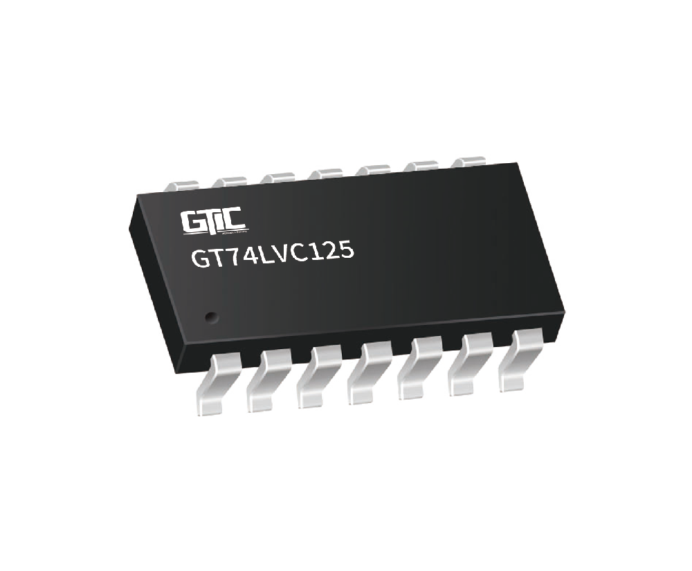
GT74LVC125
The operating voltage range of the bus buffer gate is 1.65-V to 5.5-V. The GT74LVC125 device contains quadruple buffer drivers with a 3-state output. The output is disabled when the output-enable (OE) input is high. To ensure the high-impedance state during power up or power down, OE should be tied to VCC through a pullup resistor; the minimum value of the resistor is determined by the current-sinking capability of the driver. This device is fully specified for partial-power-down applications using Ioff. The Ioff circuitry disables the outputs, preventing damaging current backflow through the device when it is powered down.
特性
- 3-State output
- Separate OE for all 4 buffers
- Wide supply voltage range from 1.65 to 5.5V
- Inputs accept voltages to 5.5 V
- Max tpd of 4.7 ns at 3.3 V
- ±24-mA output drive at 3.3 V
- Ioff ssupports partial-power-down mode
应用
- Cable modem termination system
- Video communications system
- High-speed data acquisition and generation
- Military: radar and sonar
- Motor control: high-voltage
- Power line communication modem
- SSD: Internal or external
- Video broadcasting and infrastructure
- Video broadcasting
- WiMAX and wireless infrastructure equipment


